Interaction
SPI: The Shared Rhythm of Machines
Why timing agreement wasn't enough, and why engineers chose to share a clock.
SPISerial ProtocolsSynchronousClock PhaseShift RegisterEmbedded Systems
1. The Limits of Asynchronous Agreement
In the exploration of UART, we observed how two independent microprocessors, each operating in their own private temporal domain, can exchange data using a single wire and a shared agreement. By setting a predetermined baud rate, the receiver can reconstruct bit boundaries simply by counting local oscillator cycles relative to the falling edge of the Start Bit. It is an elegant, minimal approach to interaction—yet it is built upon a delicate physical compromise.
This compromise becomes a bottleneck as system throughput requirements escalate. Because the asynchronous receiver relies entirely on its local clock, any physical discrepancy between the transmitter's oscillator and the receiver's oscillator accumulates over the frame. At 9600 baud, a 2% timing mismatch is inconsequential; the sample point drifts only slightly away from the bit's center. But if we attempt to scale the transfer rate to 10 Mbps or 20 Mbps, a fraction of a microsecond of phase drift translates into multiple bit periods of misalignment, causing catastrophic corruption.
To combat this drift, asynchronous frames must remain short—typically restricted to 8 payload bits. Consequently, a substantial portion of the bandwidth is consumed by non-data overhead: start bits, stop bits, and idle gaps. For every byte sent, at least two framing bits must be transmitted, yielding an automatic 20% protocol tax. When a system needs to transfer megabytes of image data to a display, or pull raw high-frequency sensor readings, this framing overhead and timing sensitivity make the asynchronous model physically untenable.
2. Shifting the Burden: The Shared Clock
To break past the speed limits of asynchronous protocols, embedded engineers had to rethink the nature of time itself. Instead of requiring the receiver to reconstruct time, why not transmit time directly along with the data?
This shift in thinking is the core of Synchronous communication, and it is the foundation of the Serial Peripheral Interface (SPI). By adding a dedicated physical line—the Serial Clock (SCLK)—the transmitter takes on the responsibility of orchestrating the timing of the entire bus. The receiver no longer needs to guess where a bit begins or ends, nor does it need to count local clock ticks. It simply watches the SCLK wire: when the clock line transitions, the receiver samples the data line. When the clock line is idle, the system waits.
This physical synchrony immediately eliminates the threat of oscillator drift. Because the clock line dictates the timing of the data transitions, the bus speed can scale from zero to tens of megahertz without phase misalignment. If the master processor pauses mid-transmission to handle an interrupt, the clock simply stops, the state of the bus freezes in place, and the transfer resumes later without a single bit of corrupted data. Time becomes a physical signal, not an expectation.
3. The Four Wires of the Bus
To achieve this high-speed, synchronous coordination, SPI establishes a strict Master-Slave hierarchy. Unlike UART's symmetric point-to-point architecture, an SPI bus always operates under the absolute control of a single Master device. The master generates the clock signal and drives the conversation. The Slave devices are passive, reacting only to the clock and signal boundaries initiated by the master.
The physical interface consists of four dedicated lines, each serving a distinct architectural role:
• SCLK (Serial Clock): Driven exclusively by the master, this line carries the pulse train that synchronizes data shifts and samples across all connected devices.
• MOSI (Master Out Slave In): The data line driven by the master to transmit payload bits to the slave.
• MISO (Master In Slave Out): The data line driven by the slave to transmit payload bits back to the master.
• CS / SS (Chip Select / Slave Select): An active-low control line used by the master to address and enable individual slaves. Holding the CS line low selects the target slave and wakes its interface logic; pulling it high disconnects the slave's MISO driver into a high-impedance (tri-state) mode, isolating it from the shared bus.
The schematic below illustrates how these four lines form the baseline interface between a master and a single slave device:
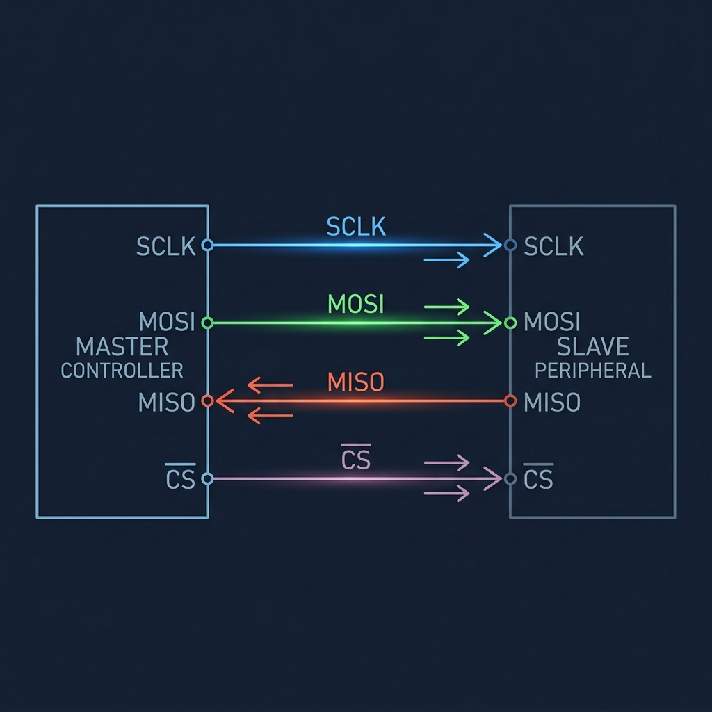
SPI Master-Slave Bus Interface Topology
4. The Shift Register Loop: Continuous Exchange
In many protocols, write operations and read operations are separate events, separated by direction changes and state handshakes. SPI, however, approaches data exchange with a unique hardware-level elegance. At its silicon core, an SPI transaction is not a separate write and read; it is a simultaneous circular swap.
Both the master and slave contain an internal shift register—typically 8 bits wide. When the master initiates a transaction, these two registers are physically connected in a closed circular loop via the MOSI and MISO lines. As SCLK toggles, the master shifts its most significant bit (MSB) out of its register onto the MOSI line, where it is shifted into the least significant bit (LSB) of the slave's register. Simultaneously, the slave shifts its MSB out onto the MISO line, where it enters the master's LSB.
After exactly 8 clock pulses, the two bytes have completely swapped places. What was in the master is now in the slave, and what was in the slave is now in the master. Every SPI write is also a read, and every SPI read requires a write. If the master only wants to read a byte from an external flash memory, it must shift out a dummy byte to generate the clock cycles required to pull the slave's data in.
This circular data loop is illustrated below, showcasing the hardware shift register interaction during a transfer:
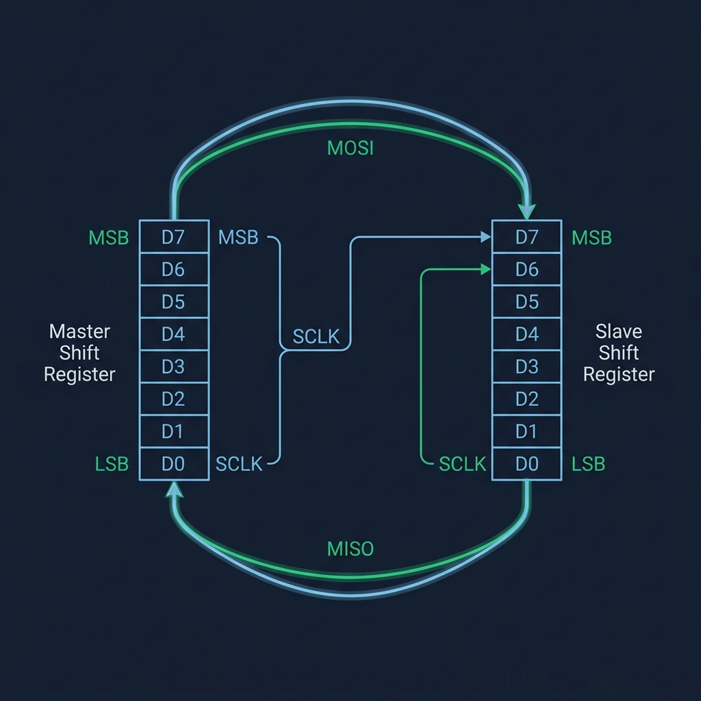
SPI Full-Duplex Shift Register Loop
5. CPOL and CPHA: The Choreography of Sampling
Because SPI is a raw hardware-level interface without a predefined standard, different slave devices require different timing alignments. Some chips expect data to change when the clock rises and be sampled when the clock falls. Others require the exact opposite. To accommodate these differences, SPI defines two configurable parameters that dictate the clock's timing behavior: Clock Polarity (CPOL) and Clock Phase (CPHA).
CPOL defines the idle state of the clock line when no communication is active:
• CPOL = 0: SCLK idles at Low (0V). The active phase of the clock consists of rising edges, and the trailing phase consists of falling edges.
• CPOL = 1: SCLK idles at High (3.3V/VCC). The active phase of the clock consists of falling edges, and the trailing phase consists of rising edges.
CPHA defines which clock transition is used to shift data vs. which edge is used to sample it:
• CPHA = 0: Data is sampled on the first (leading) edge of SCLK, and shifted out onto the line on the second (trailing) edge. This mode requires that the transmitter places the first data bit on the line the moment CS is pulled low, before the first clock edge even occurs.
• CPHA = 1: Data is shifted onto the line on the first (leading) edge of SCLK, and sampled on the second (trailing) edge.
By combining these two parameters, engineers can configure the interface in one of four distinct SPI Modes (0, 1, 2, or 3). The timing diagram below demonstrates how these configurations adjust the relationship between SCLK transitions and the MOSI/MISO data windows:
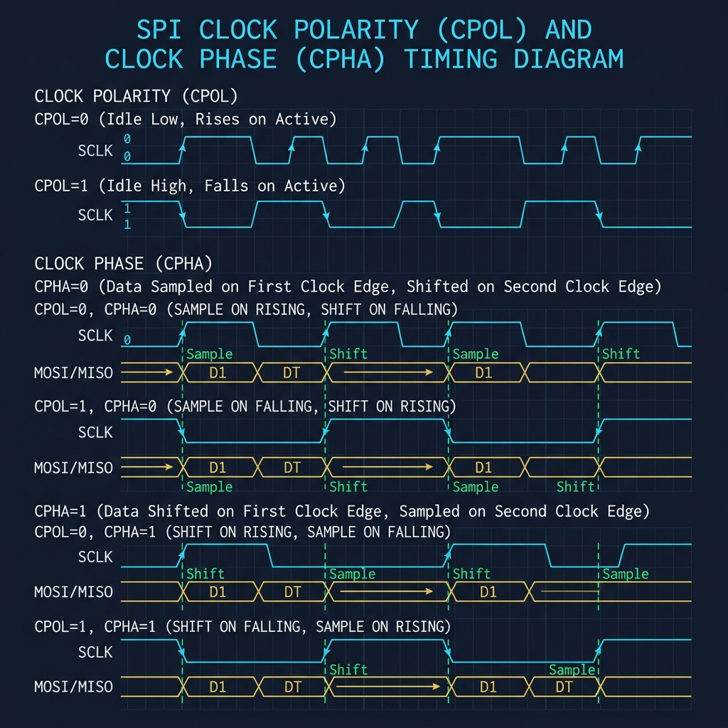
SPI Timing Diagram illustrating CPOL and CPHA configuration modes
6. Bus Expansion and the Chip Select Problem
Unlike network protocols that use digital addresses embedded inside data packets, SPI addresses devices physically. If a master wishes to communicate with multiple slave devices on a shared bus, it can do so in one of two configurations: independent slave routing or daisy-chaining.
In the independent configuration, the master shares the SCLK, MOSI, and MISO lines across all slaves, but routes a dedicated, individual Chip Select (CS) line to each chip. To speak to Slave A, the master pulls CS_A low while keeping CS_B high. This isolates Slave B's MISO pin, preventing it from driving the shared trace and causing bus contention. While this configuration is incredibly fast and simple to route, it suffers from severe pin inflation: adding a fourth slave requires adding a fourth IO pin to the master.
In the daisy-chain configuration, the master routes a single CS and SCLK to all slaves, but loops the MISO of one slave into the MOSI of the next, forming one giant, multi-byte shift register loop. While this saves IO pins, it introduces timing delays, as the master must shift data through every single slave in the chain to update a single register, and requires that all slaves support daisy-chain formatting in their silicon.
Physical addressing introduces silent bugs. If a glitch or transient voltage spike pulls a CS line low when it should remain high, multiple slaves will attempt to drive the MISO trace simultaneously. This results in bus contention, creating excessive current draw, heating, and corrupted data—a silent failure state that cannot be detected by the protocol itself since SPI lacks any built-in error detection or flow control.
7. The Trade-Offs of Raw Speed
SPI's dominance in high-speed, low-level embedded interfaces stems from its simplicity. Because it is synchronous, it has no start or stop bits, yielding 100% data throughput efficiency. Because it has dedicated TX and RX pins, it supports true full-duplex communication. There is no addressing overhead, no arbitration delays, and no complex state machines in silicon, allowing SPI peripherals to be incredibly small, cheap, and fast.
However, this simplicity comes at a cost:
• Pin Inflation: Every additional slave requires a dedicated CS pin in independent mode. A bus with six sensors quickly consumes nine microcontroller pins, cluttering the PCB layout and exhausting register space.
• No Flow Control: SPI is a 'blind' protocol. The master drives SCLK regardless of whether the slave is ready, busy, or has crashed. If the slave cannot process incoming bits fast enough, data is silently overwritten in its shift register.
• No Error Checking: Unlike UART, which supports optional parity bits, or CAN, which uses CRC checksums, SPI contains no built-in mechanism to verify data integrity. If electrical noise distorts a bit on the wire, the receiver registers the wrong value without warning.
8. The Coexistence of Two Worlds
Despite these limitations, SPI remains the undisputed standard for high-bandwidth embedded peripherals. When a microcontroller needs to write thousands of pixels to a color LCD, pull megabytes of firmware from a Serial Flash memory chip, or stream high-fidelity audio samples, SPI's raw speed—often exceeding 50 MHz—is essential.
UART taught us that two independent nodes can communicate through a mutual agreement on time. SPI showed us that by sharing a clock physically, we can discard the timing contract and unlock speeds orders of magnitude higher. But as embedded systems grew more complex, containing dozens of small sensors, displays, and controllers on a single board, the pin inflation of SPI's multi-wire bus became an intolerable physical constraint.
Engineers were faced with a new design challenge: How do we retain the speed benefits of a shared clock, but route the entire system using only two wires, regardless of how many devices are connected? This design tension would eventually drive the creation of I2C—a protocol that trade-offs raw speed to achieve absolute pin efficiency.
The Synchronization Rhythm
In the design of digital interfaces, speed is a function of synchrony. When we share a clock, we share a pulse, allowing data to flow at the speed of silicon state transitions.
SPI survives because it is the ultimate expression of raw hardware-level communication: fast, simple, and unburdened by protocol overhead.
A shared clock is a shared heartbeat. When systems beat to the same rhythm, they no longer need to discuss when to speak.
Current Exploration
SPI: The Shared Rhythm of Machines
